


250W PWM inverter circuit SG3524.
A 250W PWM inverter circuit built around
IC SG3524 is shown here. SG3524 is an integrated switching regulator
circuit that has all essential circuitry required for making a switching
regulator in single ended or push-pull mode. The built in circuitries
inside the SG3524 include pulse width modulator, oscillator, voltage
reference, error amplifier, overload protection circuit, output drivers
etc. SG3524 forms the heart of this PWM inverter circuit which can
correct its output voltage against the variations in the output load. In
a non PWM inverter the change in output load directly affects the
output voltage (when output load increases output voltage decreases and
vice versa), but in a PWM inverter the output voltage remains constant
over a range of output load.
Circuit diagram of 250W PWM inverter.
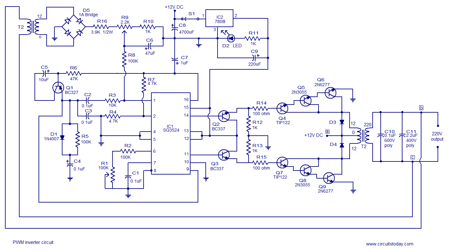
About the circuit.
Resistor R2 and capacitor C1 sets the
frequency of the ICs internal oscillator. Preset R1 can be used for fine
tuning of the oscillator frequency. Pin 14 and pin 11 are the emitter
terminals of the internal driver transistor of the IC. The collector
terminals of the driver transistors (pin 13 and 12) are tied together
and connected to the +8V rail (output of the 7808). Two 50Hz pulse
trains which are 180 degree out of phase are available at pin 14 and 15
of the IC. These are the signals which drive the subsequent transistor
stages. When signal at pin 14 is high, transistor Q2 is switched on
which in turn makes transistor Q4, Q5, Q6 ON are current flows from the
+12V source (battery) connected at point a (marked with label a) through
the upper half of the transformer (T1) primary and sinks to ground
through the transistors Q4, Q5 and Q6. As a result a voltage is induced
in the transformer secondary (due to electromagnetic induction) and this
voltage contributes to the upper half cycle of the 220V output
waveform. During this period pin 11 will be low and its succeeding
stages will be inactive. When 11 of the IC pin goes high Q3 gets
switched ON and as result Q7, Q8 and Q9 will be also switched ON.
Current flows from the +12V source (marked with label a) through the
lower half of the transformer primary and sinks to the ground through
transistors Q7, Q8, Q9 and the resultant voltage induced at the T2
secondary contributes to the lower half cycle of the 220V output wave
form.
The output voltage regulation section of
the inverter circuit works as follows. The inverter output (output of
T2) is tapped from point’s labelled b, c and supplied to the primary of
the transformer T2. The transformer T2 steps down this high voltage ,
bridge D5 rectifies it and this voltage ( will be proportional to the
inverter’s output voltage) is supplied to the pin1 (inverting input of
the internal error amplifier of the IC) through R8, R9, R16 and this
voltage is compared with the internal reference voltage. This error
voltage will be proportional to the variation of the output voltage from
the desired value and the IC adjusts the duty cycle of the drive
signals ( at pin 14 and 12) in order to bring back the output voltage to
the desired value. Preset R9 can be used for adjusting the inverters
output voltage as it directly controls the amount of voltage fed back
from the inverter output to the error amplifier section.
IC2 and its associated components
produce an 8V supply from the 12V source for powering the IC and its
related circuitries. Diodes D3 and D4 are freewheeling diodes which
protect the driver stage transistors from voltage spikes which are
produced when the transformer (T2) primaries are switched. R14 and R15
limit the base current of Q4 and Q7 respectively. R12 and R13 are
pulldown resistors for Q4 and Q7 which prevents their accidental switch
ON. C10 and C11 are meant for bypassing noise from the inverter output.
C8 is a filter capacitor for the voltage regulator IC 7808. R11 limits
limits the current through the indicator LED D2.
Notes.
- Mount the SG3524 on a holder.
- All capacitors other than C10 and C11 must be rated at least 15V.
- Preset R9 can be used for adjusting the inverter’s output voltage.
- Preset R1 can be used for adjusting the inverter’s operating frequency.
- Transistors in the driver stage require heatsink.
- T2 is a 220V primary, 12V secondary, 1A transformer.
- T1 is a 12-0-12 V primary, 220V secondary, 300VA transformer.
- Driver transistors must be isolated from the heatsink using mica sheets. Mounting kits for these transistors are easily available in the market.
- An optional finned aluminium heatsink can be attached to the 7808.
- If 1A bridge is not available, make one using four 1N4007 diodes.


1 comments:
My Testimony Hello everyone. Am here to testify how I got my loan from Mr. Benjamin after I applied several times from various loan lenders who promised to help but they never gave me the loan. Until a friend of mine introduced me to Mr.Benjamin Lee promised to help me and indeed he did as he promised without any form of delay.I never thought there are still reliable loan lenders until I met Mr. Benjamin Lee, who indeed helped with the loan and changed my belief. I don't know if you are in any way in need of a genuine and urgent loan, Be free to contact Mr. Benjamin via WhatsApp +1-989-394-3740 and his email: 247officedept@gmail.com thank you.
Post a Comment